According to the market research giant Mordor Intelligence, the global semiconductor bonding market is projected to grow from USD 1.19 billion in 2026 to USD 1.45 billion by 2031, registering a 4.04% CAGR (Compound Annual Growth Rate). Industry growth is being supported by rising investments in advanced packaging technologies, particularly chiplet-based designs and 3D integration.
“Die-to-die bonding accounts for 53.91% of interconnect-related revenue, reflecting the industry’s shift toward heterogeneous integration for improved performance and manufacturing efficiency. In addition, government-backed semiconductor programs worth more than USD 80 billion across major economies are accelerating capacity expansion and driving demand for next-generation bonding solutions,” Mordor stated in its report.
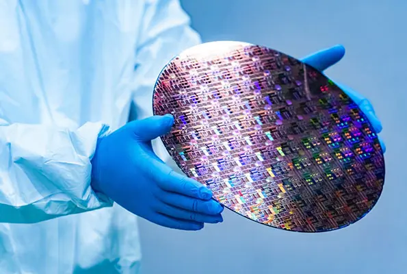
The rapid development of artificial intelligence (AI) and edge computing applications is accelerating the use of heterogeneous integration and advanced semiconductor packaging. Companies are combining multiple chip functions within a single package to achieve faster data processing, lower latency, and improved energy efficiency. This evolution is creating strong demand for high-precision bonding technologies.
“As semiconductor packaging requirements continue to evolve, stakeholders are placing greater emphasis on dependable market intelligence grounded in consistent research standards and transparent analysis. Mordor Intelligence combines structured industry coverage, rigorous data validation, and balanced assessment of market developments, helping decision-makers evaluate opportunities with greater confidence than reports that rely on narrower datasets or less comprehensive methodologies,” said Himanshu Vasisht, Senior Research Manager, Mordor Intelligence.
One of the key challenges for the industry is the substantial investment needed for advanced bonding equipment and production infrastructure. High setup costs, ongoing maintenance expenses, and lengthy return-on-investment periods can limit adoption, particularly among smaller manufacturers and assembly providers.
“As semiconductor devices continue to shrink and become more sophisticated, bonding processes are becoming increasingly complex. Maintaining precise alignment, ensuring high yields, and meeting strict quality standards require advanced expertise and process control. These technical challenges can slow implementation and increase production costs across the industry,” Vasisht concluded.